AD8219
Rev. A | Page 10 of 12
THEORY OF OPERATION
AMPLIFIER CORE
In typical applications, the AD8219 amplifies a small differential
input voltage generated by the load current flowing through
a shunt resistor. The AD8219 rejects high common-mode vol-
tages (up to 80 V) and provides a ground referenced, buffered
output that interfaces with an analog-to-digital converter (ADC).
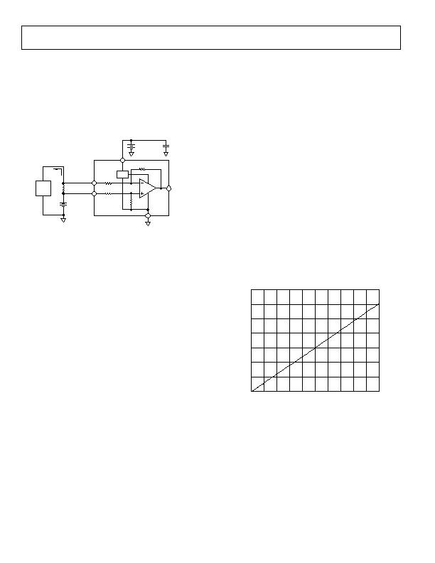
Figure 26 shows a simplified schematic of the AD8219.
LDO
R2
R1
AD8219
R4
R3
+IN
V
S
IN
OUT
GND
LOAD
V
2
I
LOAD
V
1
SHUNT
4V
TO
80V
GND
4V TO 80V
Figure 26. Simplified Schematic
The AD8219 is configured as a difference amplifier. The
transfer function is
OUT = (R4/R1) ?(V1 V2)
Resistors R4 and R1 are matched to within 0.01% and have
values of 1.5 M?and 25 k? respectively, meaning an input
to output total gain of 60 V/V for the AD8219, while the
difference at V1 and V2 is the voltage across the shunt resistor
or VIN. Therefore, the input-to-output transfer function for the
AD8219 is
OUT = (60) ?(VIN)
The AD8219 accurately amplifies the input differential signal,
rejecting high voltage common modes ranging from 4 V to 80 V.
The main amplifier uses a novel zero drift architecture, providing
the end user with breakthrough temperature stability. The offset
drift is typically less than ?00 nV/癈. This performance leads
to optimal accuracy and dynamic range.
SUPPLY CONNECTIONS
The AD8219 includes an internal LDO, which allows the user
to connect the VS pin to the inputs, or use a separate supply at
Pin 2 (VS) to power the device. The input range of the supply
pin is equivalent to the input common-mode range of 4 V to
80 V. The user must ensure that V
S
is always connected to the
+IN pin or a separate low impedance supply, which can range
from 4 V to 80 V. The V
S
pin should not be floating.
OUTPUT CLAMPING
When the input common-mode voltage in the application is
above 5.6 V, the internal LDO output of the AD8219 also
reaches its maximum value of 5.6 V, which is the maximum
output range of the AD8219. Because in typical applications
the output interfaces with a converter, clamping the AD8219
output voltage to 5.6 V ensures the ADC input is not damaged
due to excessive overvoltage.
OUTPUT LINEARITY
In all current sensing applications where the common-mode
voltage can vary significantly, it is important that the current
sensor maintain the specified output linearity, regardless of
the input differential or common-mode voltage. The AD8219
maintains a very high input-to-output linearity even when the
differential input voltage is very small.
0.7
0
0.1
0.2
0.3
0.4
0.5
0.6
0
1
9
8
7
6
5
4
3
2
1
DIFFERENTIAL INPUT VOLTAGE (mV)
0
Figure 27. Typical Gain Linearity at Small Differential Inputs
(V
CM
= 4 V to 80 V)
Regardless of the common mode, the AD8219 provides a
correct output voltage when the input differential is at least
1 mV. The ability of the AD8219 to work with very small
differential inputs, regardless of the common-mode voltage,
allows for optimal dynamic range, accuracy, and flexibility in
any current sensing application.
发布紧急采购,3分钟左右您将得到回复。
相关PDF资料
ADL5317ACPZ-REEL7
IC CURRENT MONITOR 16LFCSP
ADM1027ARQZ-RL7
IC REMOTE THERMAL CTLR 24QSOP
ADM1029ARQZ-R7
IC SENSOR 2TEMP/FAN CTRL 24QSOP
ADM1030ARQZ-RL7
IC SNSR TEMP/FAN PWM CTRL 16QSOP
ADM1032ARZ-REEL
IC TEMP MONITOR 85DEG 8SOIC
ADM1033ARQZ-RL7
IC THERM/FAN SPEED CTLR 16-QSOP
ADM1034ARQZ-REEL
IC THERM/FAN SPEED CTRLR 16-QSOP
ADN8810ACPZ-REEL7
IC CURRENT SOURCE(12BIT) 24LFCSP
相关代理商/技术参数
AD821AQ
制造商:未知厂家 制造商全称:未知厂家 功能描述:Voltage-Feedback Operational Amplifier
AD821BQ
制造商:未知厂家 制造商全称:未知厂家 功能描述:Voltage-Feedback Operational Amplifier
AD821JN
制造商:未知厂家 制造商全称:未知厂家 功能描述:Voltage-Feedback Operational Amplifier
AD821JR
制造商:未知厂家 制造商全称:未知厂家 功能描述:Voltage-Feedback Operational Amplifier
AD821KN
制造商:未知厂家 制造商全称:未知厂家 功能描述:Voltage-Feedback Operational Amplifier
AD821SQ
制造商:未知厂家 制造商全称:未知厂家 功能描述:Voltage-Feedback Operational Amplifier
AD822
制造商:AD 制造商全称:Analog Devices 功能描述:Single-Supply, Rail-to-Rail Low Power FET-Input Op Amp
AD822_06
制造商:AD 制造商全称:Analog Devices 功能描述:Single-Supply, Rail-to-Rail Low Power FET-Input Op Amp